
Ipod Video LCD hacking
More LCD hacking here
Looking for a small, cheap LCD for a possibly large-scale project, I decided that the
2.5" QVGA TFT in the Ipod Video may be worth a look, as cheap clones of it are
available from Hong Kong via Ebay..
Not finding any info on this unit on the net, I decided to investigate myself, &
bought a faulty ipod on Ebay to dissect. The hard disk was dead, but I could get it into service test
mode, which was all I needed to fiddle with the display to see how it was driven.
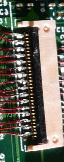
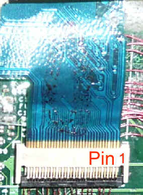
First problem was that the connector is a 0.3mm pitch FFC, so somewhat fiddly to
connect to...... but I'm not easily defeated by fiddliness, and have a really good magnifier..
The FFC connector is staggered, with pins on alternate sides, so the wires soldered on to
it are 0.6mm apart. I also needed to keep them very tidy & flat to stop them fouling
the flex cable entry and locking lever.
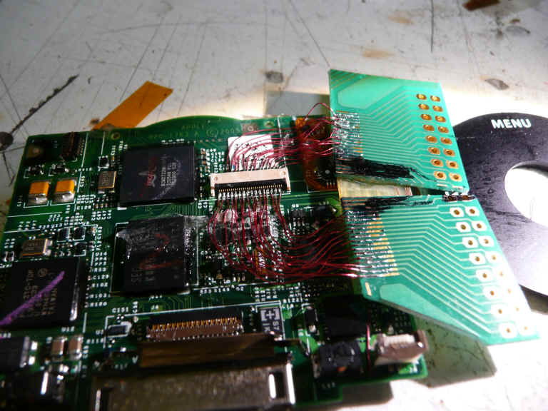
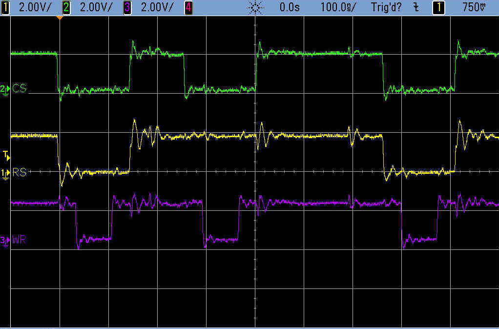
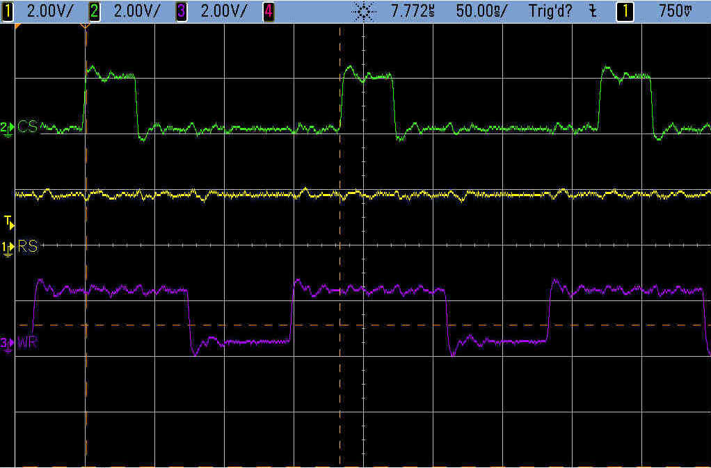
I'd been reading a few controller datasheets, so had a good idea of what I was looking for. After identifying the power and ground pins, some probing with the scope pretty soon found what looked like the control lines - WR,RD,CS,RS. This left exactly 16 more signals - the data bus.
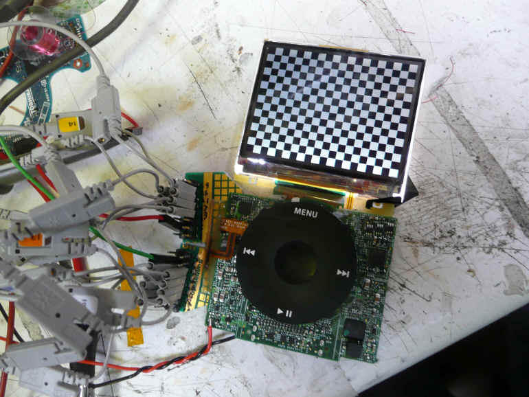
A major stroke of luck was that the test mode had some screen tests which displayed a
graduated scale from black to each primary colour, so the RGB values counted upwards
through the frame. This made identifying which pins mapped to R,G,B pretty trivial :
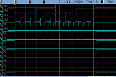
I assumed that the bus was mapped from D0..15 along the pins, and this appears to be
confirmed by looking at the commands sent at the start of a frame, which contained values
corresponding to the 320x240 resolution ( see later)
Took a while to find the connector manufacturer - it's a 32 way 0.3mm pitch ZIF FFC - and unusually has an even number of pins and reverse-side latch. Couldn't find it from HRS,JAE, JST or Molex. Then I noticed the connector on the hard disk had a similar style of latch, so looked up the HD on the Toshiba site & found a datasheet listing the connector manufacturer. It's a DDK FF12 series, part number FF12-32A-R11A. I've also seen an Omron part used on another ipod PCB, and it looks like the part number should be XF2B-3245-31A, but the datasheet for this series doesn't list a 32 way option.
I enquired with a DDK distributor about availablility, and found that the minimum order
is not just one reel, which I sort of expected, but three (7500 connectors), at GBPŁ0.71
each.
I think I'll have to see if it's feasible to use a more readily available 33 pin
connector.....
| Connector pinout (I've called pin 1 as shown above - nearest the edge of the LCD frame) | ||
| Pin | Function | |
| 1 | Not Used | |
| 2 | 3.1V Supply | |
| 3 | 1.8V Presumably I/O supply. All I/Os run at 1.8v
levels. hopefully this pin can be set to 3V or 3.3v for 3V IO - I'll wait til I have ID'd the controller, or have an expendable display before testing this! |
|
| 4 | 0V | |
| 5 | /Reset. | |
| 6 | /CS Chip select | |
| 7 | /WR write strobe | |
| 8 | RS Selects command/data register ( called CD in some datasheets) | |
| 9 | /RD read strobe | |
| Data bus | Colour | |
| 10 | D0 | Blue 0 |
| 11 | D1 | Blue 1 |
| 12 | D2 | Blue 2 |
| 13 | D3 | Blue 3 |
| 14 | D4 | Blue 4 |
| 15 | D5 | Green 0 |
| 16 | D6 | Green 1 |
| 17 | D7 | Green 2 |
| 18 | 0V | |
| 19 | D8 | Green 3 |
| 20 | D9 | Green 4 |
| 21 | D10 | Green 5 |
| 22 | D11 | Red 0 |
| 23 | D12 | Red 1 |
| 24 | D13 | Red 2 |
| 25 | D14 | Red 3 |
| 26 | D15 | Red 4 |
| 27 | 0V | |
| 28 | Vsync out. Goes high for 84.5us at frame rate of 47Hz | |
| 29 | 0V | |
| 30 | Backlight - | |
| 31 | Backlight + Vf is 13.7V ( 4 white LEDs in series) | |
| 32 | Not used | |
Next step is to try to identify the controller. One way will be to look at the commands and try to match with possible chips for which I have data. But will post a few requests on the net to see if anyone already knows.... It should be possible to figure out how to drive it without the data, by logging the commands, but there may be some more interesting features that can be used once the controller is identified.
If you know for sure what controller this LCD uses, please let me know!
The register structure looks similar to the Toshiba JBT6K71, but registers are used that do not exist on that part, so best guess so far is it's another one in the Toshiba range.
possibles ( not checked yet) : JBT6K98,
Eliminated so far : JBT6K71, R61503, LDS285,S6D0154,ILI9320,S1D19122,JBT6K74A,JBT6K85,
Initialisation sequence
Start of initialisation - Burst at end of trace is main initialisation sequence shown below. The six pulses inbetween are writes of 0000 with RS low.
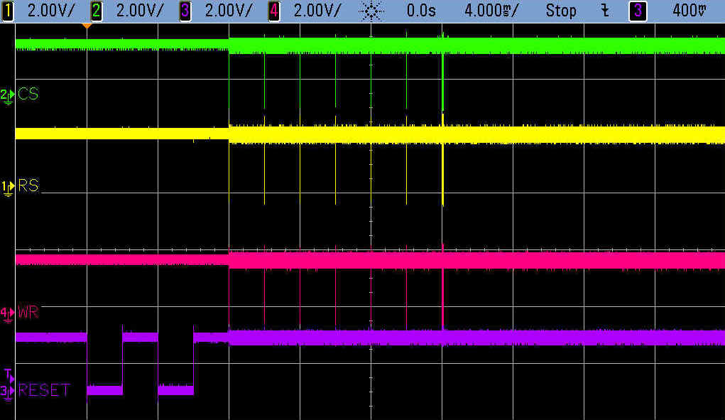
Start of main initialisation
b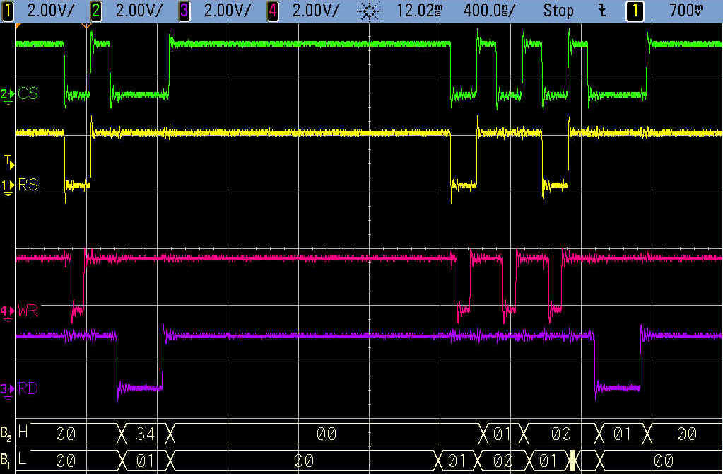
| Initialisation sequence | ||
| Write 00 with RS low | ||
| Read with RS high - returns 3401 - probably
device type identifier (It is possible that the firmware supports multiple controller types based on this ID....) |
||
| Commands in the list below consist of : Write
of address with RS low, then write of data with RS high. The first of these (write of 0100 to 0001 is shown in the trace above.
|
||
| Address (hex) | Data ( hex) | Function |
| 0001 | 0100 | |
| 0002 | 2500 | |
| 0003 | 02b0 | |
| 0004 | 0000 | |
| 0008 | 0404 | |
| 0009 | 0000 | |
| 000b | 0000 | |
| 000d | 00b4 | |
| 0010 | 0018 | |
| 0011 | 2600 | |
| 0012 | 2200 | |
| 0013 | 0802 | |
| 0014 | 080c | |
| 0015 | 0816 | |
| 0016 | 2200 | |
| 0031 | 0000 | |
| 0080 | 0031 | |
| 0400 | 001d | The sequence up to & including this write is repeated on powerdown |
| 0300 | 0705 | |
| 0301 | 0006 | |
| 0302 | 0302 | |
| 0303 | 0303 | |
| 0304 | 0300 | |
| 0305 | 0103 | |
| 0306 | 001f | |
| 0307 | 0705 | |
| 0308 | 0006 | |
| 0309 | 0302 | |
| 030a | 0303 | |
| 030b | 0300 | |
| 030c | 0203 | |
| 030d | 001f | |
| 0401 | 0001 | |
| 0007 | 0001 | |
| 0205 | 0060 | |
| 0110 | 0001 | |
| 0100 | 15b0 | |
| 0101 | 0020 | |
| 0102 | 029d | |
| 0103 | 0e5b | |
| 0105 | 0103 | |
| 0106 | 0103 | |
| 0007 | 0021 | |
| 0102 | 02bd | |
Sequence on powerdown (Power to LCD is removed on switchoff, so this command may not be to put display in powerdown mode!)
| Steps 0001 to 0400 above, then : | ||
| 0007 | 0032 | ? power control? |
Sequence when writing new frame of image data
| Command ( write with RS low) | Data ( write with RS high) | Function |
| 0210 | 0000 | First X co-ordinate of window to write |
| 0211 | 013f | Second X co-ordinate of window to write |
| 0212 | 0000 | First Y co-ordinate of window |
| 0213 | 00ef | Second Y co-ordinate of window |
| 0200 | 0000 | ?( these two commands are listed as 'write RAM address' in JBT6K71A datasheet) |
| 0201 | 0000 | ? |
| 0202 | Write-data command ( JBT6K71A data lists as data read/write) | |
| <RGB data> | ||
Access timing - command
Access timing - Data - rate is 5.5MHz. Full frame write takes 14.2mS
Driving it youself.
This display should be drivable from most microcontrollers ( *I've not yet verfied that it can do 3.3v I/O. If not, you'll need alot of resistors, or a level shifter), however the 16 bit data bus will need rather alot of I/O pins. If you're running from something like a NXP LPC2xxx ARM processor, this may not be a big deal, and you may want the speed of the 16 bit bus.
However there are a couple of simple ways to cut down the number of I/O pins needed, at the cost of extra components, and speed. They also assume you're using the display in write-only mode, and so would not be suitable if, for example, you wanted to read out the display RAM contents. A write-only interface could leave RD tied high ( assuming the initialisaiton sequence doesn't require the read - seems unlikely). You might also be able to tie CS and WR together.
1) 8 bit latch. Use an 8 bit I/O port to drive the bottom 8 data
lines. Connect an 8 bit latch like a 74HC574 with its inputs to the 8 bit port, and the
outputs to the top 8 bits of the display's data bus. Connect the latch clock to
another I/O pin. To write a 16 bit value, output the MSbyte to the port, wiggle the clock
pin, then output the LSbyte and wiggle the LCD's CS/WR pins.
You should be able to share the latch clock with WR to avoid needing an extra IO pin - the
HC574 will latch data on the rising edge, so the LCD module will ignore the latch
pulse when CS is high, and the latch data will have been read by the LCD when WR goes high
after the write with CS low.
2) Shift register. Use two 8-bit shift registers, e.g. 74HC164, driven from a SPI port ( could use normal IO but a hardware SPI port will usually be faster) - clock 16 bits of data into the registers to set up the required value on the display databus, then twiddle the LCD CS/WR lines to do the write. As above, if you're short of pins, you could share a pin between the shift clock and WR, and use the data out to drive the RS line, so you'd only need 4 lines in total ( clock+WR, data+RS, CS, Reset)